-
 20 Oct 2025 • Journal Article • ACS Photonics
Waveguide Integrated Self-Powered MoS2 Photodetectors in the Shortwave Infrared Wavelengths


 Abstract
Broadband photodetectors (PDs) are essential for various applications, including optical communication, sensing, and imaging. Modern semiconductor PD technologies often face challenges related to spectral coverage, power consumption, complex manufacturing, and limited integration with silicon electronics. As photonics technologies continue to advance alongside growing
… show more
 copied!
 -
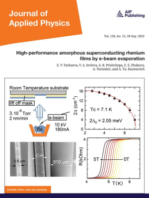 28 Sep 2025 • Journal Article • Journal of Applied Physics
Enhancing ferroelectrics with insulators: Band offsets at the Al2O3/BaTiO3 interface


 Abstract
Engineering ferroelectric interfaces is key to improving device performance. Combining thin insulators with ferroelectrics is a promising approach for minimizing leakage currents and increasing the switching efficiency. In this work, we study the interface between atomic layer deposited amorphous Al2O3 and epitaxial BaTiO3 films. These materials constitute simple and
… show more
copied! -
 2 Sep 2025 • Journal Article • Physical Review Letters
Mixing of Surface and Bulk Optical Nonlinearities via Surface Plasmon Polaritons


 Abstract
We present controlled interplay between the surface second-order and bulk third-order nonlinearities of gold, utilizing wave mixing between surface plasmons on the metal-air interface and free-space photons. By tuning the nonlinear interactions, we demonstrate experimentally that photons emerging from these inherently different mechanisms can interfere, while both their
… show more copied!
 -
 21 Jul 2025 • Journal Article • Applied Physics Letters
Velocity and temperature dependent adhesion and friction in mesoscale graphite contacts


 Abstract
The weak interlayer binding in two-dimensional layered materials such as graphite has been the subject of intensive experimental investigation and modeling for structural superlubric and electronic devices. Yet, the effects of sliding velocity and temperature on the interfacial lateral forces in mesoscale contacts are poorly understood. Here, we report experiments of
… show more
copied! -
 18 Jun 2025 • Journal Article • The Journal of Physical Chemistry Letters
Controlling Intramolecular Vibrational Redistribution with an Infrared Photonic Cavity

 Abstract
Using ultrafast dual-frequency two-dimensional infrared spectroscopy (DF-2DIR), we probed how the strong coupling of high-frequency molecular vibrations to surface lattice resonances of infrared antennas, which act as a photonic cavity, affects intramolecular vibrational relaxation (IVR). DF-2DIR allows one to probe the IVR pathways beyond the vibrational state subspace
… show more
copied! -
 16 Jun 2025 • Journal Article • Advanced Intelligent Systems
Ultrathin (<10 nm) Electrochemical Random-Access Memory that Overcomes the Tradeoff between Robust Weight Update and Speed in Neuromorphic Systems
 Abstract
Electrochemical random-access memory (ECRAM) devices are a promising candidate for neuromorphic computing, as they mimic synaptic functions by modulating conductance through ion migration. However, the use of a thick electrolyte layer (>40 nm) in conventional ECRAMs leads to an unavoidable tradeoff between synaptic weight updates and operating speed. To address this
… show more
copied! -
 20 May 2025 • Journal Article • ACS Applied Optical Materials
Exciton Manipulation via Dielectric Environment Engineering in 2D Semiconductors
 Abstract
Two-dimensional (2D) semiconductors are promising for photonic applications due to their exceptional optoelectronic properties, including large exciton binding energy, strong spin–orbit coupling, and potential integration with the standard complementary silicon-oxide-semiconductor (CMOS) technology. The dielectric environment can significantly affect the photoluminescence
… show more
copied! -
 18 May 2025 • Conference Paper • 2025 IEEE International Memory Workshop (IMW)
Novel Ultrafast Non-Destructive Readout of FeRAM by Low-Voltage Transient Current


 Abstract
Conventional FeRAM readout methods are destructive, requiring polarization switching of the FE capacitor (FeCAP) and write-back, which reduces endurance, increases latency, and energy consumption. Prior works on non-destructive readout (NDRO) relied on capacitance memory window (MW), which is slow and requires asymmetric FeCAP structure, compromising retention and
… show more
copied! -
 3 May 2025 • Journal Article • Npj 2D Materials and Applications
Andreev pair injection into a transition metal dichalcogenide monolayer


 Abstract
We demonstrate Andreev pair injection across Nb-WS2 junction evident as Andreev reflection in differential conductivity spectra below Nb critical temperature \({T}_{c}\). The superconducting- 2D semiconducting junction defined by a focused ion beam, shaped Nb pads, and semi-dry transfer of single layer CVD-grown WS2 crystals ensured the mechanical integrity of the 2D
… show more
copied! -
 29 Apr 2025 • Preprint • arXiv
Tracking the Evolution of Near-Field Photonic Qubits into High-Dimensional Qudits via State Tomography


 Abstract
Quantum nanophotonics offers essential tools and technologies for controlling quantum states, while maintaining a miniature form factor and high scalability. For example, nanophotonic platforms can transfer information from the traditional degrees of freedom (DoFs), such as spin angular momentum (SAM) and orbital angular momentum (OAM), to the DoFs of the nanophotonic
… show more
copied!